
They want the glass plate that carries the chip pattern to be twice as wide. On 7 September 2026, ahead of SPIE BACUS in Monterey, ASML and TSMC formed a collaborative industry initiative to push the semiconductor industry from today's 6-inch photomasks to 12-inch photomasks for High NA extreme ultraviolet lithography. The press notes that followed on the 8th — Hsinchu and Veldhoven for ASML and TSMC, Korea and the Netherlands for Samsung, Monterey and Business Wire for Intel Foundry — aren't three separate product launches. They're one ecosystem argument, told from three foundry seats.
High NA EUV ships first on the mask format the industry already knows. A larger mask is the planned second act. The dates on that second act run to 2031 for a pilot line and 2033 for full lithography-system readiness for advanced-node production.

If you've never sat through a lithography briefing, start here. What a photomask is. Why extreme ultraviolet light matters. What numerical aperture does to resolution and to the size of the exposure field. Why stitching shows up in the same sentences as High NA. Why a 12-inch — often written 6×12-inch — mask is the industry's answer to stitching. Then the three company notes in order: ASML and TSMC's initiative, Intel Foundry's production claim, Samsung's DRAM High NA plan. Quotes stay as the primaries printed them.
What a photomask actually is
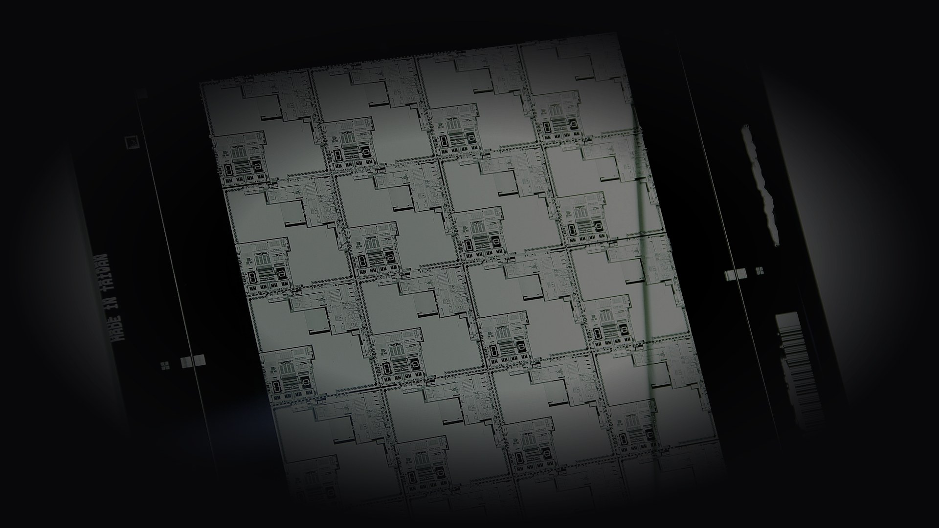
A photomask — also called a reticle in a lot of fab speech — is a glass plate that carries the pattern for one lithography layer of a chip. Think of it as a precision stencil that never touches the wafer. Light from the scanner passes through, or reflects off, the patterned mask and projects a reduced image of that pattern onto a resist-coated silicon wafer. One layer might be a metal interconnect. Another might be a gate. Another might be a contact hole. Modern processors and memory chips need dozens of such layers. Each critical layer needs its own mask, or a set of masks, that the scanner can load, align, and expose over and over.
The industry's standard mask format for leading-edge work has been a 6-inch square blank for a long time — roughly 152 millimetres on a side in the physical blank, before you get into patterned area and pellicles and all the tooling that surrounds it. That size isn't a fashion choice. It's infrastructure. Mask writers write at that size. Inspection tools inspect at that size. Stockers, pods, automation hands, and electronic design automation assumptions all grew up around it. When ASML and TSMC say "transition to 12-inch photomasks," they aren't talking about a slightly thicker glass. They're talking about changing the physical format that every station in the mask-to-scanner chain has to accept.
Why change it at all? Because High NA EUV, on the current 6-inch format, shrinks the exposure field on the wafer. That's a physics trade, not a marketing slogan. Higher numerical aperture buys finer resolution. On the same mask blank, that finer optics package delivers a smaller printable field. Large dies then need more than one exposure to cover their area — the practice the industry calls stitching. Larger masks are the proposed way to restore a full field, cut the stitching tax, and raise scanner productivity.
Why EUV showed up in the first place
For decades, chipmakers patterned wafers with deep ultraviolet light — DUV — at wavelengths such as 193 nanometres. As transistors got smaller, DUV kept going by stacking tricks: immersion lenses, multiple patterning, ever-more-complex mask stacks. Those tricks work. They also cost cycle time, process complexity, and overlay risk. Extreme ultraviolet lithography uses light at 13.5 nanometres. That shorter wavelength is the point. It lets a single exposure print features that would otherwise need several DUV passes.
EUV isn't magic light. It's a system. The light source is a tin-plasma laser-produced source. The optics are mirrors, not glass lenses, because most materials absorb EUV rather than transmit it. The mask is reflective. The scanner lives in vacuum. ASML's NXE platform — the workhorse EUV tools now common in advanced fabs — uses a numerical aperture of about 0.33. That 0.33 NA EUV generation is what the industry means when it says "Low NA" or "standard EUV" in contrast to High NA.
High NA is the next optics step on that same EUV wavelength. ASML's EXE platform pushes numerical aperture to about 0.55. Higher NA means the system can resolve finer pitches at the same wavelength, or print given pitches with more process margin. That's why foundries chasing the densest logic and the densest memory layers care about it. It's also why the mask-format conversation arrives in the same week as High NA progress notes. Optics and field size are coupled.
Numerical aperture, without the fog
Numerical aperture is a number that describes how wide a cone of light the lens — or, for EUV, the mirror system — can collect and focus. In lithography, resolution scales roughly with wavelength over NA. Shorter wavelength helps. Larger NA helps. EUV already cut the wavelength. High NA increases the aperture.
There's a cost. In a reduction scanner, the mask pattern is demagnified onto the wafer. High NA optics, on today's 6-inch mask, yield a smaller exposure field on the wafer than the Low NA NXE field. Industry shorthand for that High NA field on a 6-inch mask is often "half field" relative to the older full field. Exact millimetre figures vary by tool generation and by how you count printable area. The operational fact is enough: some dies that fit in one Low NA exposure don't fit in one High NA exposure on a 6-inch mask. Designers then either floor-plan inside the smaller field, or stitch.
That's the fork Intel Foundry named in plain language this week. Customers can use High NA with the current mask format either by floor-planning within the 6-inch mask or by using Intel Foundry's stitching capabilities and process design kit solutions. ASML and TSMC's joint release makes the complementary point: High NA will be adopted for production first on current 6-inch masks; larger 12-inch masks are expected to increase fab productivity, lower chipmaking costs, and remove stitching constraints.
What stitching is
Stitching means exposing adjacent half-fields and joining them so a larger die can be built from more than one exposure. On paper it sounds tidy. In a fab it's a tax. You spend extra exposure time. You spend overlay budget at the seam. You spend process-control attention on the join. You spend design-kit and EDA work to make the join legal for the product you're shipping.
SPIE week put stitching on the conference clock. ASML's Jan van Schoot was listed for "Scanner and mask requirements to support half field stitching" on Tuesday 8 September at 11:00 a.m. Pacific time. Intel Foundry's Kimberly Pierce was listed for "High NA EUV: stitching for manufacturing" at 11:20 a.m. in the same session. Those titles are the public record of what the two companies chose to teach this week. They're talks about making stitching work on today's mask format — not talks that declare stitching free.
Secondary coverage sometimes quotes specific wafers-per-hour drops when High NA moves from a full-field story to a half-field story. Those numbers aren't in the ASML/TSMC, Intel, or Samsung primaries. Throughput matters. Overlay matters. Availability matters. Intel Foundry's note says overlay, throughput, and availability are meeting its expectations for the High NA work already in high-volume manufacturing — without publishing a wafers-per-hour table. That's the ceiling for numbers here.

Why "12-inch" and why "6×12-inch"
The initiative language slides between "12-inch photomasks," "large-format photomasks," and "6×12-inch mask." Read them as the same family of change. Today's standard blank is a 6-inch-class square. The proposed large format roughly doubles one dimension — a 6-by-12-inch class plate — so the patterned area can support a restored full exposure field under High NA optics. "Twice as wide" in the headline is that dimensional claim in newspaper English, not a claim that every linear measure on the tool doubles.
What does the industry say the larger mask buys? ASML and TSMC's joint release is explicit: greater fab productivity, lower chipmaking costs, removal of stitching constraints, and the ability for advanced chip manufacturers to fully leverage High NA EUV so future leading-edge chips are more cost-effective. Fouquet's quote puts scanner productivity in the same breath as demand for smaller, faster, more energy-efficient chips. Chandrasekaran's Intel Foundry quote frames the near term as High NA on 6-inch masks with or without stitching, and the transition to 6×12-inch masks as the follow-on.
None of that happens by swapping one glass plate in isolation. A 12-inch mask ecosystem needs mask blanks, writers, inspection, repair, pellicles, carriers, automation, scanner stages, and EDA assumptions that all agree. That's why both the ASML/TSMC note and the Intel Foundry note keep saying "industry initiative," "ecosystem," "mask suppliers," "automation," "EDA," "materials." A single foundry can invent a stitch recipe. A mask-format change needs a crowd.
The ASML–TSMC initiative
Dateline on the joint release: Hsinchu, Taiwan, and Veldhoven, the Netherlands, 8 September 2026. Inside the release: on 7 September, in advance of the SPIE BACUS Conference, ASML and TSMC formed a collaborative industry initiative to drive the transition to 12-inch photomasks, maximizing the value of High NA EUV lithography.
Targets, as printed: establish a 12-inch mask pilot line by 2031; support full lithography system readiness for advanced node production by 2033.
Adoption sequence, as printed: High NA EUV will be adopted for production using current 6-inch masks first. The transition to larger 12-inch masks is expected to further increase fab productivity, lower chipmaking costs, and remove stitching constraints.
TSMC's High NA manufacturing intention, as printed: TSMC intends to use ASML's High NA technology in high-volume manufacturing for advanced nodes starting in 2030. As nodes advance, TSMC expects the number of layers requiring High NA EUV will rise, driven primarily by the increasingly complex transistor architectures required for AI applications.
Industry-support line, as printed: High NA EUV adopters and other major suppliers have expressed their interest to join the initiative. Major ecosystem partners and suppliers attended the 7 September event and expressed interest in the transition. Named joiners arrive in the Samsung note.
Christophe Fouquet, ASML president and CEO, on the sequence:
"We expect the adoption of High NA EUV to increase progressively along the device scaling roadmap, first using current 6-inch masks and then further supported by 12-inch masks, which enable greater scanner productivity and allow the industry to meet the demand for smaller, faster and more energy-efficient chips."
And on support:
"We are pleased by the strong initial support of semiconductor manufacturers, mask suppliers and partners for this initiative."
TSMC Chairman and CEO Dr. C.C. Wei:
"We have always believed that when the industry works together to solve complex problems, we unlock possibilities that no single company could achieve alone. By bringing together expertise from across the industry's value chain, we hope to keep providing the benefits of cutting-edge technology through continuous innovation that lowers barriers and puts advanced solutions accessible at scale."
Read Wei's sentence against the mask-format problem and it stops being ceremonial. No single company owns blanks, writers, inspection, scanners, and EDA. The initiative is a coordination claim. The dates — 2031 pilot, 2033 readiness — are the coordination clock.
Intel Foundry: High NA already in volume, on 6-inch
Intel Foundry's newsroom note is dated Monterey, California, 7 September 2026. The Business Wire version on intc.com carries a release stamp of 8 September 2026, 2:03 a.m. EDT. Same substance. The lead claim isn't a future pilot. It's present-tense manufacturing.
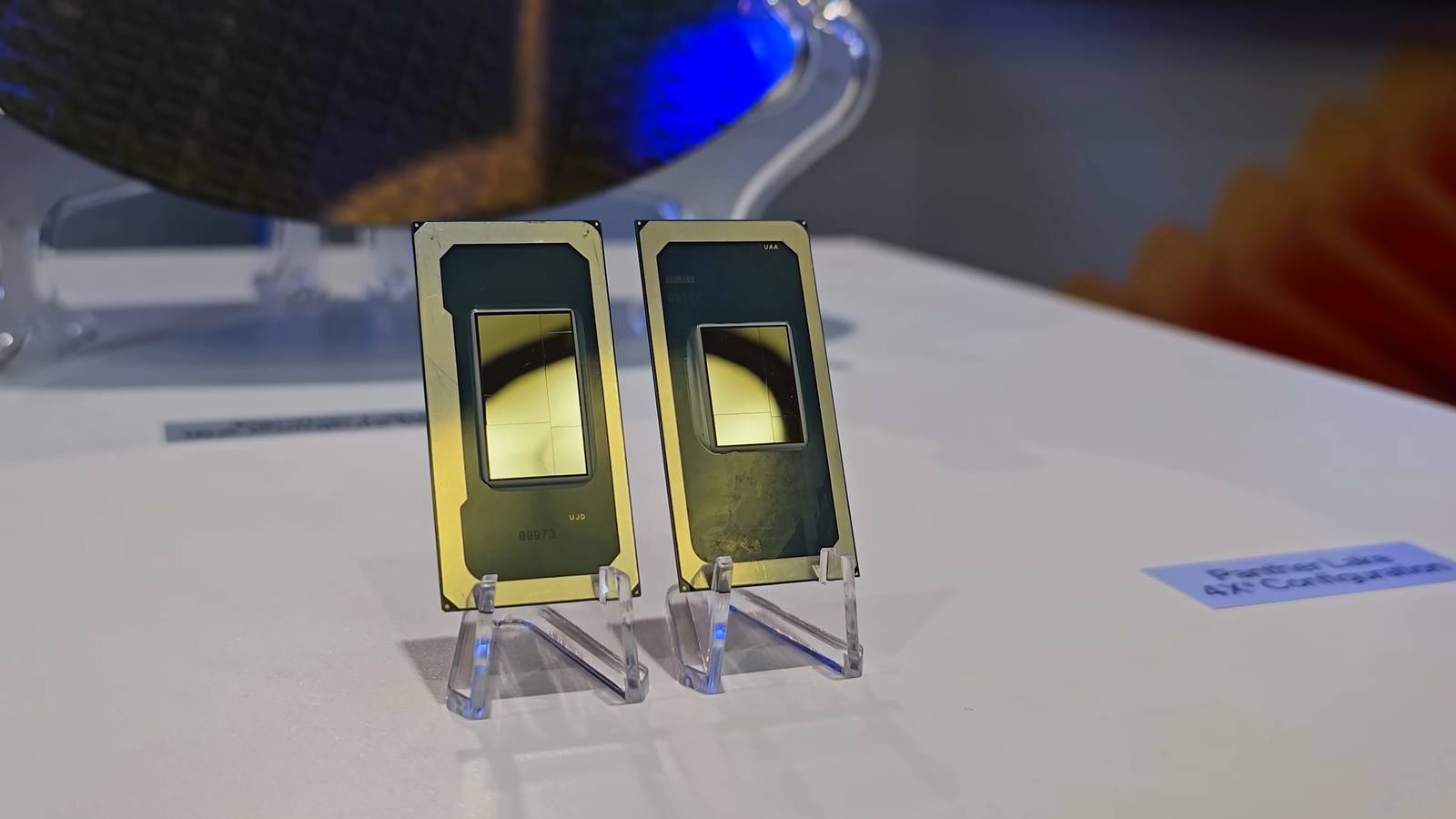
High NA continues to be used in high-volume manufacturing production at Intel Foundry today, the company says, with more than one million wafers processed to date across early tool certification and testing, research and development efforts, and volume production on select layers for a subset of Intel Core Ultra Series 3 processors, code-named Panther Lake. Overlay, throughput, and availability are meeting Intel Foundry's expectations.
That "more than one million wafers" is the only wafer-count primary in these notes. It covers certification, R&D, and volume production on select layers for a subset of Panther Lake — not a claim that every Panther Lake layer or every Intel wafer sees High NA. Select layers. Subset of the product line. Meeting expectations on overlay, throughput, availability.
On Intel 18A, the same note says products manufactured using High NA for select layers continue to deliver performance that meets or exceeds comparable layers patterned using the NXE platform — EUV with numerical aperture of 0.33. That's a comparison claim inside Intel's own process family, not a cross-foundry benchmark table.
On customer enablement with today's mask: floor-planning within the 6-inch mask, or Intel Foundry stitching plus PDK solutions. On the large-mask campaign: for more than three years, Intel Foundry has championed the large mask format initiative to align the mask ecosystem, working closely with ASML, mask makers, automation suppliers, EDA partners, materials providers, and semiconductor manufacturers.
Fouquet, speaking in the Intel note about Intel's High NA role:
"Intel Foundry has been one of the key leaders of the industry's adoption of High NA, from installing the first commercial EXE system in 2024, to qualifying the latest generation of tools, to shipping the first high-volume logic product manufactured with High NA. ASML recognizes Intel Foundry's pioneering role in High NA and its innovations to deliver value today with 6-inch masks, as well as its long-time support of the 6x12-inch mask evolution."
Naga Chandrasekaran, Intel Executive Vice President and Co-General Manager of Intel Foundry:
"The companies building the increasingly complex AI products of the future need manufacturing innovations that are production-ready and easy to use. Within our lithography capabilities, Intel Foundry is focused on near term enablement of High NA on 6-inch masks with or without stitching, and making the transition to 6x12-inch masks. We will continue to work closely with ASML and the entire industry to enable this transition."
Two clocks sit next to each other after you read that. Intel's clock: High NA value now, on 6-inch, with stitching available when a die needs it. The industry's large-mask clock: pilot 2031, system readiness 2033. Chandrasekaran's sentence holds both without pretending they're the same year.

Samsung joins the 12-inch initiative, aims DRAM High NA by 2028
Samsung Electronics and ASML published a separate strategic-collaboration note from Korea and the Netherlands on 8 September 2026. Two facts from that note matter here.
First: Samsung joins the industry initiative for a 12-inch photomask platform for High NA EUV. That's a named joiner under the tent ASML and TSMC described in general terms the same week.
Second: Samsung plans to introduce ASML High NA EUV into future DRAM high-volume manufacturing for the first time in the industry by 2028. The same note says High NA EUV is expected to extend the DRAM scaling roadmap, with improved resolution enabling process simplification and increased efficiency.
Put that against TSMC's 2030 High NA HVM intention for advanced logic nodes and Intel's present-tense High NA logic production on select Panther Lake layers. Memory and logic aren't the same product roadmaps. Samsung's 2028 DRAM claim is a memory first. TSMC's 2030 line is advanced-node logic manufacturing intention. Intel's million-wafer claim is logic layers already running. Three different verbs on three different calendars. Don't mash them into one "everyone ships High NA in year X" sentence.
Young Hyun Jun, Vice Chairman and CEO, Samsung Electronics:
"The AI era is transforming the semiconductor industry and increasing the importance of technological innovation across the entire value chain. Samsung is committed to maintaining leadership in advanced semiconductor manufacturing, including memory and foundry, through breakthrough technologies and strong partnerships. By further strengthening our collaboration with ASML, we are helping lay the foundation for the next generation of AI and semiconductor innovation."
Christophe Fouquet again, this time in the Samsung note:
"Samsung has been one of ASML's most important innovation partners for many years. Together, we have helped advance the technologies that underpin modern semiconductor manufacturing. As the industry enters a new era driven by artificial intelligence, close collaboration with our customers becomes even more important. We look forward to working with Samsung to enable the next wave of semiconductor innovation."
Fouquet appears in all three primaries this week. That isn't a coincidence of speechwriters. ASML is the common scanner vendor. The foundries are arguing, in public, about how to extract value from the same High NA platform on two mask eras.
Three notes, one table
ASML and TSMC, 7–8 September 2026: industry initiative for 12-inch photomasks; pilot line target 2031; full lithography system readiness for advanced node production 2033; High NA production first on 6-inch; TSMC High NA HVM intention from 2030; Fouquet on progressive adoption and strong initial support; Wei on industry-wide problem solving.
Intel Foundry and ASML, Monterey 7 September / Business Wire 8 September: more than one million wafers through High NA across certification, R&D, and select-layer volume production for a subset of Core Ultra Series 3 / Panther Lake; overlay, throughput, availability meeting expectations; 18A select layers meet or exceed comparable NXE-patterned layers; floor-plan inside 6-inch or stitch with PDK; three-plus years championing large mask format; Fouquet on Intel's first commercial EXE in 2024 and first high-volume logic product with High NA; Chandrasekaran on near-term 6-inch enablement and the 6×12 transition; SPIE talks by van Schoot and Pierce on stitching.
Samsung Electronics and ASML, 8 September 2026: Samsung joins the 12-inch photomask platform initiative; Samsung plans High NA EUV in future DRAM HVM by 2028, described as a first in the industry; High NA expected to extend DRAM scaling, with resolution enabling process simplification and efficiency; Jun on AI-era value-chain innovation and ASML partnership; Fouquet on Samsung as long-time innovation partner.
Shared spine: High NA value now-or-soon on 6-inch masks; large-format masks as the productivity and stitching-removal step; SPIE week as the public stage; ASML as the scanner constant; AI-driven transistor and memory complexity as the demand story the CEOs keep naming.
A short map of the trade
Start with the mask. Glass plate. Chip-layer pattern. Scanner projects it onto the wafer.
Add the light. EUV at 13.5 nanometres versus older DUV. Shorter wavelength, reflective optics, vacuum tool, reflective mask.
Add the aperture. NXE about 0.33 NA. High NA EXE about 0.55 NA. Finer resolution. Smaller field on the same 6-inch mask.
Add the workaround. Floor-plan inside the half field, or stitch half-fields together. Stitching costs time and overlay attention. It's real manufacturing, not a lab toy — Intel is teaching it at SPIE and shipping select layers — but it's still a tax.
Add the proposed fix. 12-inch / 6×12-inch masks. Restore field. Remove stitching constraints. Raise productivity. Lower cost, per the ASML–TSMC framing. Needs a whole supplier chain, which is why this is an "initiative" and not a lone purchase order.
Add the calendars. Intel: High NA HVM layers already, million-plus wafers cumulative across the categories it listed, first commercial EXE install cited by Fouquet as 2024. Samsung: DRAM High NA HVM plan by 2028. TSMC: High NA HVM for advanced nodes from 2030. Industry large-mask pilot: 2031. System readiness for advanced-node production on that format: 2033.
If someone tells you High NA isn't real yet, point them at Intel's select-layer volume claim and Fouquet's "first high-volume logic product" line. If someone tells you the mask problem is already solved, point them at 2031 and 2033. If someone collapses memory and logic into one date, separate Samsung's DRAM 2028 from TSMC's logic 2030 and Intel's present tense.
What "remove stitching constraints" means
It doesn't mean stitching disappears from every conversation the day a 12-inch blank ships. Pilot line 2031 isn't a fleet. System readiness 2033 isn't a promise that every layer of every product moves overnight. Mask-format transitions are multi-year because blanks, writers, inspection sensitivity, pellicle readiness, and scanner stages have to co-qualify.
It does mean the industry's public roadmap now treats stitching on 6-inch High NA as a bridge, not as the permanent destination. Intel's note is careful on that point: near-term enablement with or without stitching, and a transition to 6×12. ASML and TSMC are careful too: adopt High NA on 6-inch first, then support further with 12-inch. Samsung's join is a vote that the destination format matters for memory as well as logic.
Designers still have to choose, product by product, whether a die fits the High NA field, whether stitching is cheaper than a floor-plan compromise, and when a large-mask-capable scanner and mask line are actually available in the fab that will ship the part. Those choices are factory economics. The public notes this week are the scaffolding around them.
Why AI keeps showing up in the CEO quotes
TSMC's release ties rising High NA layer counts to "increasingly complex transistor architectures required for AI applications." Chandrasekaran talks about "increasingly complex AI products." Jun talks about the AI era transforming the semiconductor industry. Fouquet, in the Samsung note, talks about a new era driven by artificial intelligence.
None of those lines is a model-card claim. They're demand-side framing. AI accelerators and the memory that feeds them push density, power, and interconnect complexity. Density and interconnect complexity push lithography. Lithography at the leading edge pushes EUV layer counts. EUV layer counts at the toughest pitches push High NA. High NA on a half field pushes stitching or floor-plan limits. Stitching and floor-plan limits push the large-mask initiative. You can disagree with any CEO's emphasis. The causal chain they're sketching is coherent enough to explain why three foundry notes landed in the same SPIE week.
TSMC said the number of layers requiring High NA will rise as nodes advance. That's the verified claim. How many High NA layers a future AI GPU needs isn't in these primaries.
Monterey week as a coordination stage
SPIE Photomask Technology + Extreme Ultraviolet Lithography — BACUS in the older short name still used in the ASML–TSMC note — is where mask and EUV people already gather. Filing an industry initiative "in advance of" that conference is a way to put suppliers in one room and then put the press notes on the wire while the talks run.
The stitching session on Tuesday 8 September is the technical companion to the strategy notes. Van Schoot on scanner and mask requirements for half-field stitching. Pierce on stitching for manufacturing. If you only read the CEO quotes, you miss that the companies are also teaching the bridge technique in public. If you only read the talk titles, you miss the 2031/2033 destination dates. Read both.
Intel's note says the companies have been building the large-format path for years with mask makers, automation suppliers, EDA partners, materials providers, and semiconductor manufacturers. ASML and TSMC say major ecosystem partners and suppliers attended the 7 September event and expressed interest. Samsung says it joins. The week is a roll-call as much as it is a physics lesson.
The week in newspaper order
Monday 7 September 2026, ahead of SPIE BACUS in Monterey: ASML and TSMC form the collaborative industry initiative for 12-inch photomasks. Same Monterey frame: Intel Foundry and ASML publish the High NA production-and-stitching progress note. Tuesday 8 September: ASML–TSMC joint release on the wire from Hsinchu and Veldhoven; Samsung–ASML collaboration note from Korea and the Netherlands; Intel's Business Wire stamp in the small hours Eastern; stitching talks on the SPIE clock at 11:00 and 11:20 a.m. Pacific.
The industrial argument underneath the timestamps is simple enough to say in one breath. High NA EUV is valuable enough that Intel is already shipping select logic layers on it with today's 6-inch masks. It's valuable enough that Samsung is aiming it at DRAM high-volume manufacturing by 2028. It's valuable enough that TSMC intends it for advanced-node high-volume manufacturing from 2030, with layer counts expected to rise as transistor architectures get harder. And it's constrained enough, on a 6-inch blank, that the same companies are organizing a multi-year march to a mask twice as wide, with a pilot line targeted for 2031 and production-system readiness targeted for 2033.
Primary sources
ASML and TSMC joint press release, Hsinchu and Veldhoven, 8 September 2026 (initiative formed 7 September): https://www.asml.com/en/news/press-releases/2026/tsmc-and-asml-announce-industry-transition-to-large-format-photomasks-for-high-na-euv.
Intel Foundry newsroom, Monterey, 7 September 2026: https://www.intel.com/content/www/us/en/newsroom/news/intel-foundry/intel-foundry-asml-accelerate-industry-readiness-for-high-na-euv.html.
Intel / Business Wire release via intc.com, released 8 September 2026, 2:03 a.m. EDT: https://www.intc.com/news-events/press-releases/detail/1781/intel-foundry-and-asml-collaborate-to-accelerate-industry.
Samsung Electronics and ASML, Korea and the Netherlands, 8 September 2026: https://news.samsung.com/global/samsung-electronics-and-asml-expand-strategic-collaboration-for-next-generation-semiconductor-manufacturing.
Mask shops, scanners, and why coordination is the story
Chipmaking headlines often sound like pure physics. Wavelength. Aperture. Resolution. The mask-format story is half logistics. A mask shop has to write the larger blank without blowing write time and defect density. An inspection tool has to see the larger area at the defect sizes High NA cares about. A pellicle — if the process uses one — has to survive EUV power on a larger frame. A fab's automation has to move a heavier, differently shaped carrier without teaching every robot a new bad habit. A scanner stage has to hold and scan the larger reticle with the overlay the process needs. EDA tools have to place and check layouts against a field map that matches what the scanner will actually print.
That list is why Fouquet's "strong initial support of semiconductor manufacturers, mask suppliers and partners" line matters, and why Intel's three-year championship language lists mask makers, automation, EDA, materials, and semiconductor manufacturers in one breath. The ASML–TSMC initiative isn't a bilateral friendship announcement. It's an attempt to align that list on a public timetable.
Wei's line about unlocking possibilities no single company could achieve alone is doing the same work in TSMC's voice. Jun's line about innovation across the entire value chain is doing it in Samsung's. Chandrasekaran's "production-ready and easy to use" is the customer-facing version: a foundry can offer High NA on 6-inch with or without stitching now, while the industry builds the easier full-field path.
6-inch High NA isn't a consolation prize
It'd be easy to misread this week as "High NA doesn't count until 12-inch masks arrive." The primaries reject that reading.
Intel says High NA is in high-volume manufacturing today on select layers, with overlay, throughput, and availability meeting expectations, and with 18A select-layer performance meeting or exceeding comparable NXE layers. Fouquet credits Intel with shipping the first high-volume logic product manufactured with High NA and with innovations that deliver value today with 6-inch masks. Samsung is aiming High NA at DRAM HVM by 2028 on the roadmap it published — years before the 2031 large-mask pilot target. TSMC intends High NA HVM from 2030, again before the 2033 large-mask readiness target.
So the honest newspaper sentence is dual. High NA on 6-inch is already a production tool for at least one logic foundry's select layers, and a near-term plan for others. The 12-inch mask is the productivity and stitching-removal upgrade the same companies want the ecosystem to finish. First act and second act. Not understudy and star.
Floor-planning versus stitching
Floor-planning within the 6-inch High NA field means you accept the smaller printable area and arrange the die — or the reticle shot map — so each exposure stays inside what one High NA pass can cover. That can mean smaller chips, different multi-chip packages, or careful placement of the densest IP blocks. It avoids a stitch seam. It can constrain product definition.
Stitching means you accept the seam and spend engineering on making the seam invisible to the product's electrical and reliability requirements. That's why Pierce's talk title says "stitching for manufacturing" and why Intel pairs stitching with PDK solutions. A stitch that works in a lab photograph isn't enough. The process design kit has to make the stitch a legal, characterizable option for customers who will tape out against it.
Neither fork is cheating. Both are ways to take High NA resolution to market before the large-mask infrastructure exists at scale. The large-mask initiative is the industry admitting it'd rather not live on those forks forever for the products that want a full field.
Logic, DRAM, and why the calendars differ
Logic foundries and memory makers share lithography vendors and often share physical limits. They don't share product cadences. A CPU or AI accelerator die may be large, stitch-sensitive, and hungry for the densest middle-of-line or backend layers. A DRAM part may care about a different set of critical layers and about bit-cost economics that punish process complexity. Samsung's note says High NA's improved resolution can enable process simplification and increased efficiency on the DRAM scaling roadmap. That's a memory argument: fewer tricks, cleaner process, better efficiency — not the same sentence as TSMC's rising High NA layer counts for complex transistor architectures.
So when you see 2028 next to Samsung DRAM, 2030 next to TSMC advanced-node HVM, and "today" next to Intel select logic layers, you're seeing three product strategies hanging off one scanner platform. The 12-inch mask initiative is the rare sentence that can include all three without forcing their tape-out years to match.
What "full lithography system readiness" points at
ASML and TSMC's 2033 phrase is "full lithography system readiness for advanced node production." Read that as scanner-plus-mask-ecosystem readiness aimed at advanced-node manufacturing, not as a promise that every advanced node on earth converts on 1 January 2033. A lithography system, in ASML's world, is the scanner in a network of source, optics, stages, software, and service. "Readiness" in a press release is program-milestone language. Factories still have to buy, install, qualify, and yield.
The 2031 pilot line is earlier and narrower: a 12-inch mask pilot line. That's where blanks get written and proven at the new format before the industry trusts the format with leading-edge volume. Pilot before readiness. Readiness before whatever volume each customer actually books. Keep the order.
Fouquet across three podiums
In the TSMC joint release, Fouquet emphasises progressive High NA adoption on 6-inch then 12-inch, scanner productivity, and strong initial support. In the Intel note, he emphasises Intel's first commercial EXE install in 2024, qualification of later tools, first high-volume logic product with High NA, value on 6-inch today, and long-time support of 6×12 evolution. In the Samsung note, he emphasises a long innovation partnership and closer collaboration as AI drives a new era.
Same executive. Three audiences. The through-line matches the industrial dual clock: ship value on the mask you have; organise the mask you want next.
Four numbers to keep: more than one million wafers already processed through High NA in the categories Intel listed; Samsung DRAM High NA HVM plan by 2028; TSMC High NA HVM intention from 2030; large-mask pilot 2031 and system readiness 2033. One physical object: the photomask — the glass plate that holds the layer pattern — and the proposal to make the large-format version wide enough to give High NA its field back. One caution: stitching is real, teachable, and already part of a manufacturing offer, and it's still a constraint the industry is trying to retire with a bigger plate of glass.

The paper
Comments
No notes on this story yet.
Sign in to comment